
The 74-500 DASH (data acquisition system hardware) is used on PHI 5600 to 5800 XPS systems and comprises two circuit boards to count the MCD preamp signals. Those boards plug into a motherboard which in turn is connected to power supplies and the PC.
The DASH motherboard has connectors on both sides of the board and so it can not be flow soldered on both sides of the board. To get around that issue the motherboard was designed using square pins on the 96 pin connectors which fit tightly into some round pads on the board. The corners of the square pins make electrical contact with the pads.
Over a long period of time (20 plus years) oxidation can buildup on the square pins which result in poor electrical contact between the pins and the pads.
The result can be unstable operation of the DASH that can show up at unstable data, wide peaks and overflow count rates (over 20 million CPS).
The fix for this contact issue is to solder the pins to the pads by hand. There are a total of 576 pins that need to be soldered, it takes some time to do.
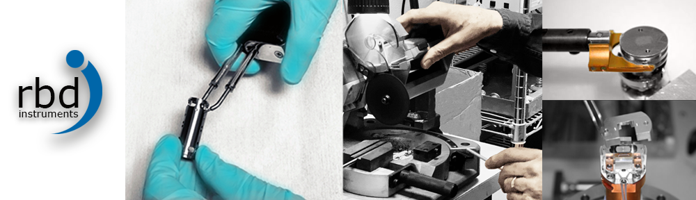
The pictures below show the back of the DASH mother board and the pins before and after soldering.
Remove the two little break out board and then solder all the pins. Clean off the flux after soldering all the pins.


Replace the breakout boards after soldering and cleaning the board. If your MCD or DASH issue is related to the DASH mother board pin contacts, soldering all of the pins on the 96 pin connectors will solve the problem.
For more information about troubleshooting count issues with the PHI 5600 to 5800 XPS systems contact RBD Instruments.


